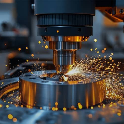
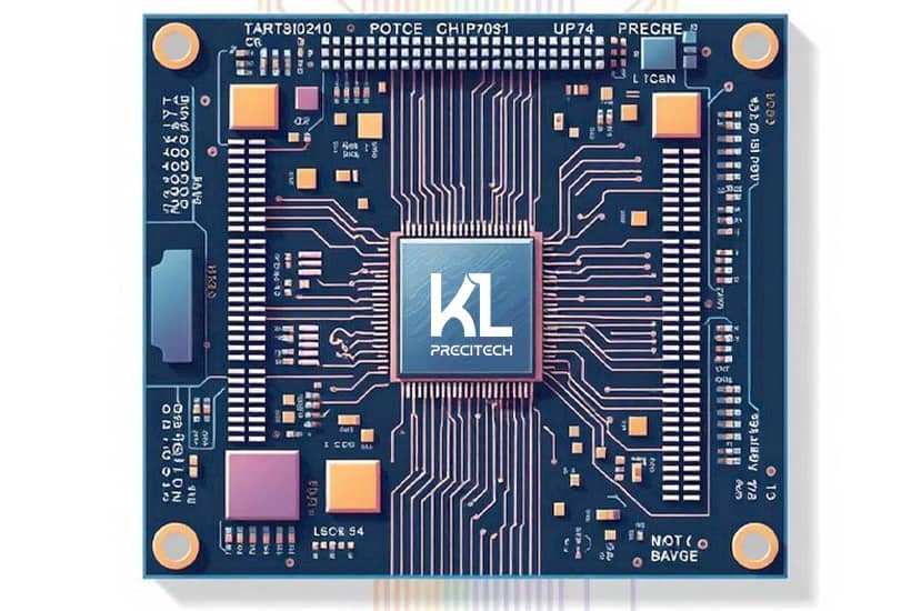
PCBA Design & Manufacturing
From Concept to Circuit — Your One-Stop Partner for PCB Design, Product Costing, Benchmarking and reverse engineering & PCBA Manufacturing.
Your Custom Prototype Manufacturing Expert
We bring your electronic ideas to life with precision engineering, transparent costing, and end-to-end manufacturing support.
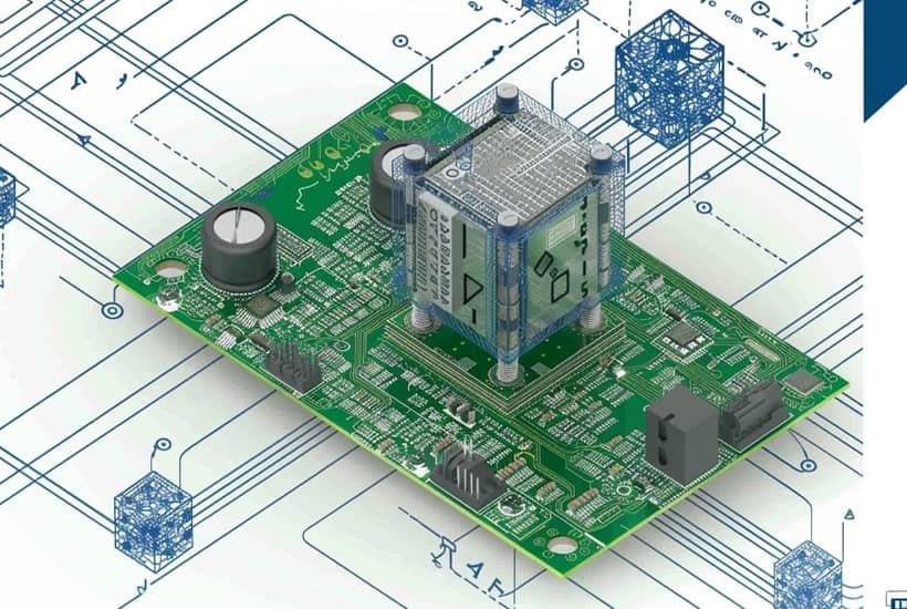
Our PCB design division focuses on creating high-performance, manufacturable, and reliable printed circuit boards tailored to each client’s unique product requirements. We handle everything — from schematic design to final Gerber release — ensuring optimal signal flow, component placement, and electrical performance.
Schematic Design & Capture
Translating your electrical concept into detailed, optimized schematics using advanced design tools like Altium Designer, OrCAD, and KiCAD.
PCB Layout &
Routing
Multi-layer board design with a focus on minimizing noise, crosstalk, and EMI. We handle complex high-speed designs, mixed-signal, and RF layouts.
Design for Manufacturing & Design for Assembly
We ensure your designs are ready for smooth fabrication and assembly without costly revisions.
Signal Integrity & Power Analysis
Simulations and validations to maintain consistent electrical performance under varying loads and environmental conditions.
Library & Footprint Management
Creation and validation of accurate component footprints and symbols as per IPC standards.

Documentation & Output Files
Complete set of Gerber, BOM, drill, pick-and-place, and fabrication drawings for manufacturing partners.
Get Free Quote
- Expert PCB Design Engineers
- Manufacturing
- Transparent Costing & Valuation
- Reverse Engineering Expertise
- Fast Prototyping to Mass Production
What We Offer
Product Costing & Valuation
Accurate costing is crucial for product success. We provide data-driven, transparent costing for electronic products, helping you make informed design and manufacturing decisions.
Our Costing Methodology Covers:
- Component-Level Cost Analysis:
Detailed breakdown of resistors, ICs, connectors, and passive components — including sourcing options and lead times. - PCB Fabrication & Assembly Costing:
Includes layer count, finish type, solder mask, copper weight, and assembly complexity. - Tooling & Fixture Cost Estimation:
For special jigs, test fixtures, or machining setups required in manufacturing. - BOM Optimization:
Alternate component recommendations for cost efficiency without compromising quality. - Import & Logistics Cost Evaluation:
For projects involving international suppliers and large-volume production. - Lifecycle Cost Analysis:
Understand how material selection, supplier stability, and design changes affect long-term profitability.
Deliverables
Detailed Cost Report (in Excel or PDF)
Comparative Vendor Quotations (if available)
Suggestions for Cost Reduction & Sourcing Alternatives
Benefits to Clients
✅ Early-stage design cost visibility
✅ Reduced procurement expenses
✅ Improved budgeting accuracy
✅ Data-backed negotiation with suppliers
OVERVIEW
Reverse Engineering & Benchmarking
We specialize in Reverse Engineering and Product Benchmarking for electronic and electro-mechanical systems.
Our expertise helps clients recreate product performance, analyze competitor devices, identify cost optimization opportunities, and upgrade designs — all while maintaining precision and compliance with industry standards.
Reverse Engineering is not just copying a product; it’s about understanding how it works, improving its performance, and optimizing it for manufacturability and cost.
- Original design data or documentation is missing or incomplete.
- Product needs upgradation or localization (e.g., import substitution or Indianization).
- Customer wants to analyze competitor products for benchmarking or performance insights.
- Legacy equipment needs maintenance, redesign, or modernization.
- Existing systems require cost optimization and improved reliability.
Step 1 – Product Assessment & Requirement Study
We begin by understanding the client’s goal—whether it involves repair, upgrade, redesign, or benchmarking. This is followed by identifying the system’s functionality, electrical characteristics, and mechanical interfaces. Finally, we plan a structured teardown and analysis procedure to ensure a thorough and efficient evaluation.
Step 2 – Physical Disassembly & Data Capture
Our process involves careful dismantling of electronic assemblies, enclosures, and connectors, followed by detailed visual inspection and photography at every stage. We use 3D scanning and high-resolution imaging to capture accurate mechanical dimensions, while also documenting electrical connections, component markings, and circuit traces for comprehensive analysis.
Step 3 – PCB and Circuit Analysis
We trace and map PCB layers using microscopic inspection or X-ray scanning for multilayer boards, enabling a clear understanding of the internal structure. This includes identifying component packages, reference designators, and overall circuit topology. Using advanced EDA tools, we generate accurate schematics and netlists, and subsequently create Gerber files and layout data to support re-manufacturing or redesign requirements.
Step 4 – Component Identification & Sourcing
We identify all electronic components, including active and passive parts, connectors, and integrated circuits, and then generate a complete Bill of Materials (BOM) with accurate manufacturer part numbers. We also suggest modern equivalents or replacements for obsolete components and provide cost comparison and sourcing support to assist in new builds or redesigns.
Step 5 – Mechanical Reconstruction
We rebuild precise 2D and 3D CAD models of housings, chassis, and fixtures using advanced 3D scanning and CAD software. This is followed by detailed checks for fit, tolerance, and alignment to ensure manufacturability and proper assembly. When required, we also perform finite element validation to assess mechanical strength and thermal performance.
Step 6 – Testing & Validation
We conduct functional testing of re-engineered PCBs and assemblies to ensure proper operation, followed by a detailed comparison of electrical parameters and performance against the original product. We also verify safety, EMI/EMC compliance, and overall operational consistency to ensure the redesigned solution meets required standards.
Step 7 – Documentation & Handover
We provide all deliverables in a comprehensive engineering report that includes detailed schematic diagrams, PCB Gerber and fabrication files, a complete Bill of Materials (BOM) with suitable alternates, and precise 2D/3D CAD models in STEP, IGES, or SolidWorks formats. The report also includes assembly drawings, mechanical interface documentation, and thorough test reports along with a benchmarking summary, ensuring complete clarity and support for manufacturing or redesign efforts.
REVERSE ENGINEERING
Product Benchmarking
Benchmarking is a key part of our reverse engineering service. It involves analyzing and comparing the design, performance, and cost parameters of competing or reference products.
- End-to-end reverse engineering from mechanical to electronic systems
- Expertise in both digital and analog domains
- In-house 3D scanning, PCB tracing, and testing capabilities
- Documentation and IP-safe approach
- Cost-effective and time-bound delivery
Technical Teardown Analysis
Disassembling competitor products to study their materials, circuits, and construction quality.
Performance Evaluation
Measuring power consumption, efficiency, thermal behavior, and functional accuracy.
Design Comparison
Evaluating architecture, layout, and component selection for optimization insights.
Cost Benchmarking
Estimating component and manufacturing costs to compare value and efficiency.
Patent & IP Consideration Support
Ensuring that reverse-engineered or benchmarked designs comply with IP boundaries and legal frameworks.
Tools & Technologies We Use
- 3D Scanning & Measurement: Faro Arm, CMM, and Laser Scanners
- EDA Software: Altium Designer, OrCAD, KiCAD
- CAD/CAM Tools: SolidWorks, AutoCAD, Fusion 360
- Testing Equipment: Multimeters, Oscilloscopes, LCR meters, Thermal Imaging Cameras
- Analysis Tools: X-Ray PCB Inspection, Solder Joint Microscopy
Key Deliverables
- Reverse-engineered design data and schematics
- PCB layout and Gerber files
- Full BOM with sourcing guidance
- 3D CAD files and assembly drawings
- Functional test and comparison report
- Benchmarking report (technical + cost comparison)
powered by precision
Our Vision for Domestic Market
India’s electronics ecosystem is growing rapidly, from EVs and defence to consumer devices, yet many startups and small manufacturers face challenges such as high MOQs and import dependency. KL Precitec fills this gap by offering a local, flexible, and supportive PCBA manufacturing ecosystem that promotes product innovation and aligns with “Make in India” goals. We focus on long-term partnerships, supporting customers from their first prototype all the way to full-scale production success.
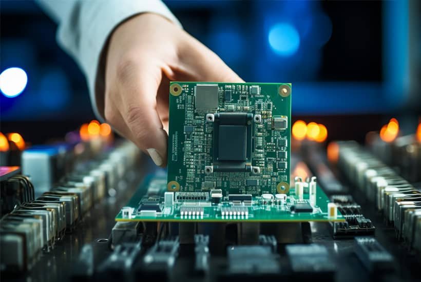
PCBA MANUFACTURING
End-to-End PCBA Manufacturing Solutions
At KL Precitec, we deliver end-to-end PCBA solutions for startups, MSMEs, and OEMs seeking reliable, cost-effective, and fast electronics manufacturing in India. As an agile small-scale unit, we specialize in flexible, customized builds that bridge the gap between prototypes and mass production. Our mission is to empower domestic innovators with high-quality, affordable assembly solutions tailored to India’s growing electronics market.
- Small-batch, quick-turn PCBA builds for R&D, startups, and pilot projects.
- Affordable and transparent costing suitable for MSME and entry-level production.
- Close technical collaboration with clients for design optimization and manufacturability.
- Local sourcing and vendor network to reduce import dependency.
- In-house testing, rework, and inspection capabilities.
Your Trusted Partner
Empowering Indian Innovation
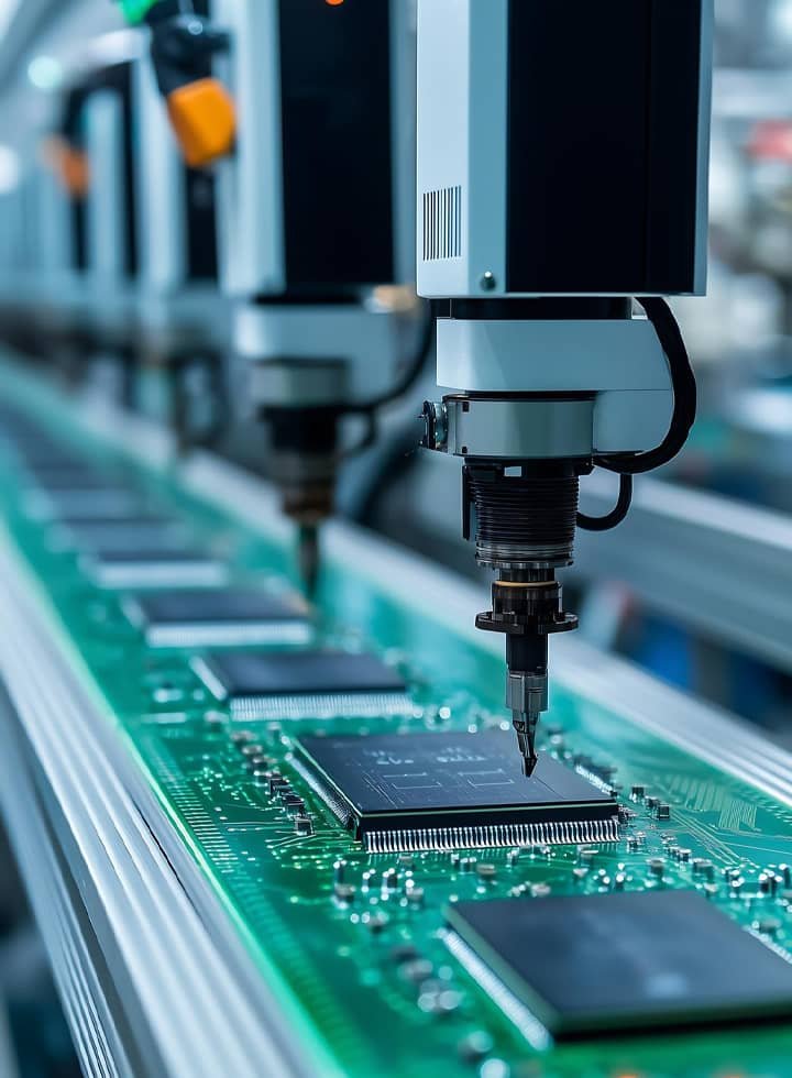
Surface Mount Technology (SMT)
- Manual and semi-automatic SMT placement for small to medium volumes.
- Reflow soldering using controlled temperature profiles for reliable joints.
- Support for components as small as 0402, SMD ICs, and connectors.
- Ideal for prototype and low-volume production runs.
Through-Hole (THT) Assembly
- Hand soldering and wave soldering for connectors, capacitors, relays, and large components.
- Skilled operators ensure clean joints and consistent quality.
- Assembly suited for power electronics, industrial controllers, and energy devices.
Mixed Technology Assembly
- Integration of SMD + THT components on the same board.
- Common for industrial control boards, motor drivers, and embedded systems.
Cable & Harness Integration
- Custom wire harness assembly, terminal crimping, and sub-assembly integration.
- Tailored solutions for EV components, sensors, and industrial applications.
Component Sourcing & BOM
- Assistance in sourcing electronic components from reliable domestic and international suppliers.
- Alternate sourcing and validation for obsolete or long lead-time parts.
- Cost optimization through BOM review and localization of supply chain.
Prototype to Production
- Seamless transition from engineering samples to regular batch production.
- Design feedback for improving manufacturability and yield.
- Scalable setup to handle increasing quantities as clients grow.
Testing & Quality Assurance
- Visual Inspection (VI) for solder joints, alignment, and polarity.
- AOI (Automated Optical Inspection) for SMD boards.
- Continuity and Power-On Testing before dispatch.
- Optional Functional Testing & Burn-in as per customer requirement.
Rework & Repair Capability
- Skilled technicians for BGA, SMD, and fine-pitch IC rework.
- Fault diagnosis and component replacement for defective PCBs.
- Quick troubleshooting for engineering revalidation.
When you partner with us, you receive:
- Fully assembled and tested PCBs (as per order volume)
- Inspection reports and test logs
- Material traceability report (on request)
- BOM and build documentation
- Support for packaging, labeling, and logistics
We cater to a wide range of domestic sectors that demand precision, reliability, and affordability:
- Defence Startups & Research Labs: Prototype and test boards.
- Electric Vehicles (EV) & Battery Management Systems: Power and control circuits.
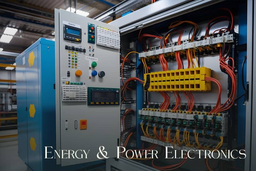
- Energy & Power Electronics: Inverters, converters, and chargers.
- Industrial Automation: Controllers, sensors, and relay logic boards.
- IoT & Consumer Devices: Compact and energy-efficient boards.


WHY CHOOSE US
Why Choose KL Precitec as Your Entry-Level PCBA Partner
- Flexible Volumes: Ideal for 10 to 1,000 PCB assemblies — perfect for pilot batches and proof-of-concept runs.
- Affordable & Transparent Pricing: Competitive costing for domestic clients without compromising quality.
- Technical Partnership: We work closely with your design team to resolve manufacturability and performance issues.
- Quick Turnaround: Fast delivery for prototype and small-batch builds.
- Local Ecosystem Support: Partnerships with PCB fabricators, enclosure makers, and component suppliers across India.
- Scalability: Ability to scale up gradually as your demand grows.
“Every idea deserves the right engineering to become real.”
Why Choose Us
Fast Engineering. Better Results.
Engineering support that moves your ideas from concept to production—faster, smarter, and with unmatched precision.
Engineered with accuracy to ensure every component meets exact standards.
Clear communication, honest timelines, and no hidden surprises.
We work closely with you to refine ideas and solve engineering challenges.
Your requirements guide every decision — from design to delivery.
Ready For A Project?
Let’s Build Your Next Breakthrough
Whether you’re developing a prototype, validating a design, or scaling toward production, our team is here to help. Share your requirements, and we’ll guide you with practical engineering insights, fast lead times, and precise execution—every step of the way.
![]()